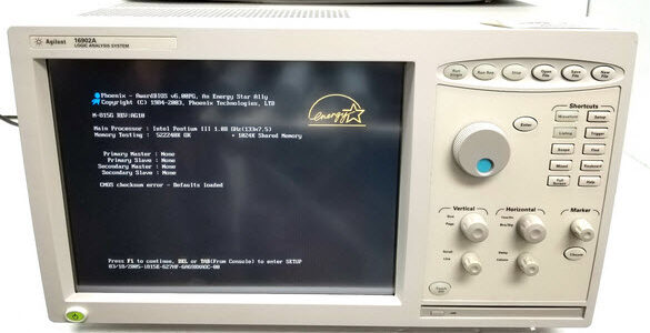
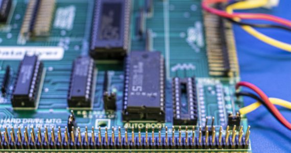
I just recently added another HP/Agilent logic analyzer to my collection. This time it is the 16902A. I needed to remove the CPU tray to replace the IDE HDD with a SATA SSD. As a result, I figured I’d take couple...
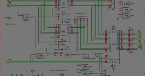
Schematics now available for A501 replacement card!
Find them on the main project page, located here.
Added some new photos of the populated PCB for the Commodore Amiga A501 memory replacement card.
Find them on the main project page here.
So the very first A500 I had been testing on since the beginning of the project had a Bug Katcher installed. It turns out that I wasn’t really using it, but I left it plugged in anyways. I’m not sure...
So I think the Amiga 500 I was testing with has problems. I’m not sure precisely what or why but Today, I dropped my new A501 replacement card into a known-working Commodore Amiga 500. It fired up immediately no...
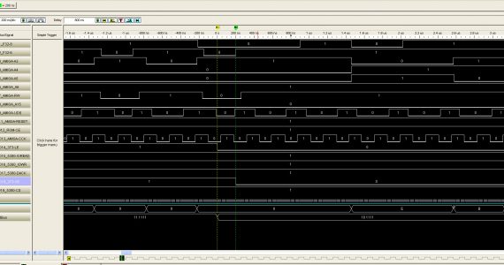
While I had my logic analyzer connected to my memory card tonight, I noticed that I no longer had the white screen hang on bootup problem that I’ve been plagued with since this card came in. As a matter of fact...
So I’ve written some assembly in the monitor software I’ve been using, and I’ve just created a large loop to see if I can get the card to fail. I’m still having plenty of problems on bootup, but...
![]()
techtravels.org is a blog that features home-grown open-source hardware and software projects.
Copyright © 2018 techtravels.org Powered by WordPress