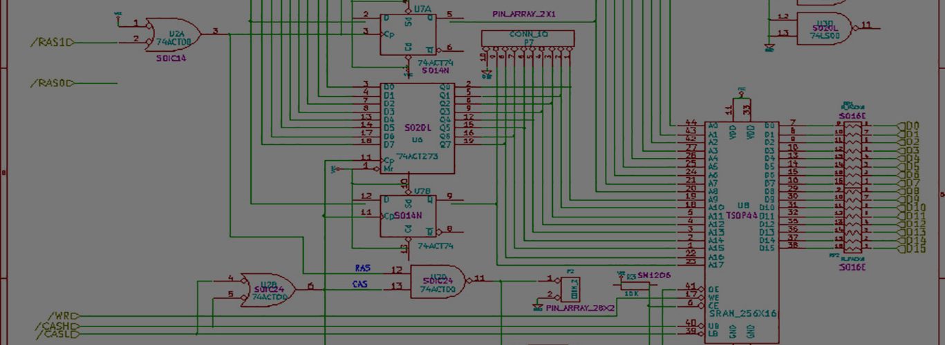
Schematics now available for A501 replacement card!
Find them on the main project page, located here.

Schematics now available for A501 replacement card!
Find them on the main project page, located here.
Added some new photos of the populated PCB for the Commodore Amiga A501 memory replacement card.
Find them on the main project page here.
So the very first A500 I had been testing on since the beginning of the project had a Bug Katcher installed. It turns out that I wasn’t really using it, but I left it plugged in anyways. I’m not sure...
So I think the Amiga 500 I was testing with has problems. I’m not sure precisely what or why but Today, I dropped my new A501 replacement card into a known-working Commodore Amiga 500. It fired up immediately no...

techtravels.org is a blog that features home-grown open-source hardware and software projects.
Copyright © 2018 techtravels.org Powered by WordPress
Very interesting read! always nice to still see ppl doing stuff with the Amiga.
I hope you will continue on expanding the memory? 🙂 How much RAM can the Amiga 500 adress in the slot-in?
The memory map allows $C00000 to $DBFFFF, which is 1,835,007 bytes. However, there have to be available address bits, driven by Agnus, to allow this happen.
So, by default, there are 18 bits of address, which gives 2^18 = 262,144 sixteen bit words. (512K of ram)
The address bus is multiplexed, so 9-bits of Row address is put on the bus, and then 9-bits of Column address on the bus.
Truthfully, I haven’t even looked into how they go about supporting more memory in the (fatter) Agnus’. They PROBABLY steal a bit or two from somewhere, but I don’t know how they actually go about getting that bit across the 56-pin memory interface connector. Because there’s no more room, or spare bits there, as far as I can tell.
A full 1.835mb would require 20 bits of address. I’d need another 2 latch bits, and of course a bigger ram chip. This would be a minor change. The hard part (of questionable hard-ness) is the glue logic, and that already works fine.
Thanks for the comment!
Ok! i understood some of the technical stuff 😉 thanks!
when i checked in winuae, you can adjust the “slow” memory to max 1,8mb ram, now i know why 😉
Why do they call it “slow” is it because of the multiplexing that makes it slower that chip ram?
Chip ram is on the motherboard, slow is in the slot-in and fast is on the side-expansion, right?
Here’s what I can tell you:
Both the onboard ram(shows up as CHIP) and the trapdoor ram(shows up as FAST) is multiplexed, both have relatively long cycle times, can have memory as slow as 120ns.
The onboard ram maps low at $0. The trapdoor maps at $C00000. You can relocate the trapdoor memory to be considered CHIP memory, which I think is done via using a 8372A Agnus.
The CPU has to be arbitrated(interleaved) through Agnus with the custom chips to be allowed access to this memory, so it can sometimes be slowed down as a result. Recent reading indicates that this can happen due to the higher resolution modes robbing the 68K cycles.
Real Fast memory is on the 68K side and is therefore directly accessible by the CPU. None of the custom chips (besides Agnus, and as far as I know) have direct access to the full 68K memory space or have access to the full address bus. They can perform I/O on the databus, but operate through “Agnus” via the smaller 8-bit RGA bus.