In order to properly reverse engineer a PAL, you need to correctly identify which pins are inputs, and which pins are outputs. This in some cases is trivial because some of the PAL’s pin functions are fixed. Let’s look at the example of a PAL16L8.
Fixed Input Pins
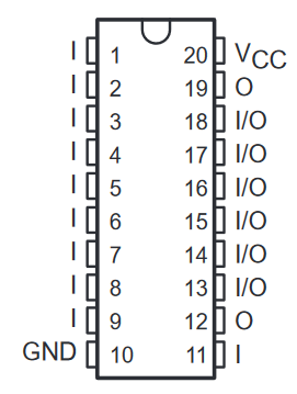
As you can see, Pins 1-9, and 11 are inputs and are fixed.
This makes it easy to define the concept of an input word. Each input pin becomes a bit in the input word, starting from the left most significant bit. While we will spend fair bit of time isolating each output bit, it’s useful to consider a collection of bits on both the input side and output side.
Or, put another way, input word + current state(if any!) = output word.
We can look at each individual unique access as a transaction to the PAL. The PAL looks at the current inputs, combines it with the current state (latched bits, for example), and then outputs. The time between the input changing, and the output asserting the new value is called the propagation delay. This propagation delay is normally something like 10ns-25ns, and is specified in the datasheet for the PAL.
You can also see where you could create a truth table of sorts, with input words in one column, and an output word in another. Assuming there truly is no state, then you can create just a simple lookup table, similar to a ROM, where you provide a 11-bit address(input word) and it spits out an 8-bit output. Remember that ROMs, including flash memory, are typically MUCH slower than the reaction time of these PALs, so NO, you probably can’t replace a PAL with a ROM. Even if there is no state.
Fixed output pins
Pins 12 and 19 in our example are fixed and will always be outputs.
The hard-er part, the IO pins, just follow the yellow brick road. (the trace!)
Pins 13 through 18 are IO pins, which means they can be configured to be input or output pins based on programming. You’ll need to look to see what they are connected to help determine the direction of the signals.
Remember that schematic I said that was so important? So let’s look at 2 pins with our example. Pin 13 and Pin 15.
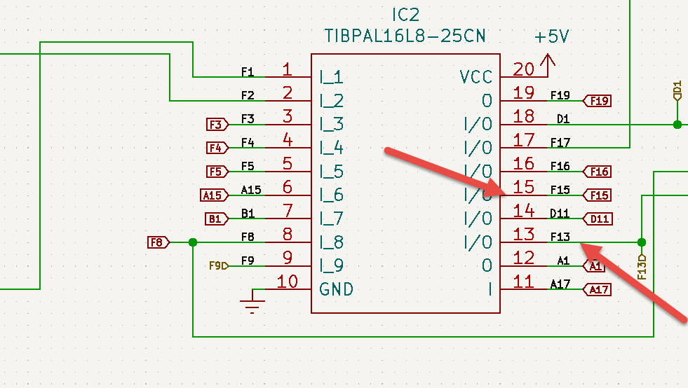
Pin 13 Investigation
Pin 13 connects with net F13 in our schematic, and Pin 15 connects to, perhaps unsurprisingly net F15.
So we’re going into KiCad and highlighting net F13:
So that connects to a card edge connector pin 16, and makes its way to the Commodore Amiga in which it’s plugged into. Checking the Amiga 500 schematic reveals
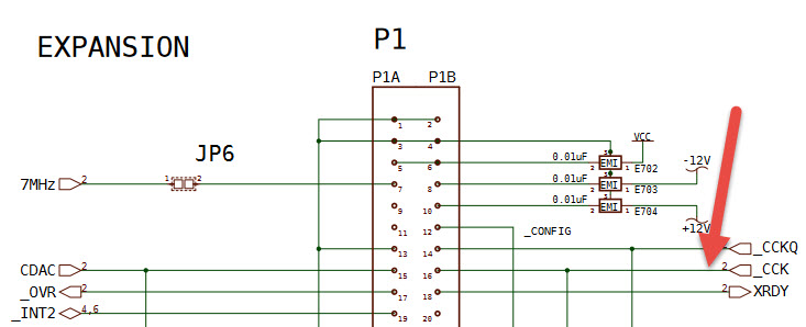
So it’s a clock, called CCK, which is generated by Agnus. So that means it’s an OUTPUT from the Amiga, and must be an input on the PAL. The arrow pointing towards the connector is also an indication that the signal is an output.
Pin 15 Investigation
So we saw Pin 15 was connected to Net F15, what’s the PCB view for that pin?
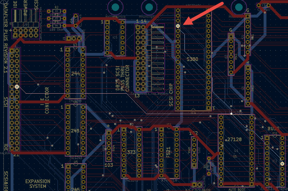
So then what’s pin 15 connected to? The SCSI chip 5380. We pull the datasheet, which we collected during our earlier Understand the System post. It connects to pin 24 on the 5380.

Lo and behold, pin 24 is an INPUT on the 5380, so it must be an OUTPUT on the PAL.
So you see it’s just a matter of reading the PAL datasheet to figure out fixed inputs and outputs, and then determining what the PAL I/O pins are connected to, and then checking the datasheet for that IC, connector, and so on.
Doing a proper job in the data collection phase makes this easy. If you’re struggling with this technique, then you haven’t collected all the information you need. Go back and re-read some the earlier posts.





Add comment